The global semiconductor landscape is witnessing a structural shift as the boundaries between chip design, fabrication, and end-use application begin to dissolve. At the center of this transition is “Terafab,” a $20 billion collaborative project recently formalized between Intel and the suite of companies led by Elon Musk, including Tesla, SpaceX, and xAI. This partnership is not merely a supply agreement; it is an industrial refactoring of how high-performance silicon is conceived and manufactured specifically for the next generation of autonomous systems and off-world data processing.
Vertical Integration at a Planetary Scale
In the world of mechanical engineering and industrial automation, the bottleneck for progress has transitioned from physical actuators and materials to the availability of specialized silicon. Tesla’s development of the Optimus humanoid robot and the Full Self-Driving (FSD) computer has long been hamstrung by the global reliance on a few concentrated fabrication points in East Asia. The Terafab project addresses this by creating a dedicated pipeline for custom Application-Specific Integrated Circuits (ASICs) that are optimized for the unique power and thermal profiles of mobile robotics.
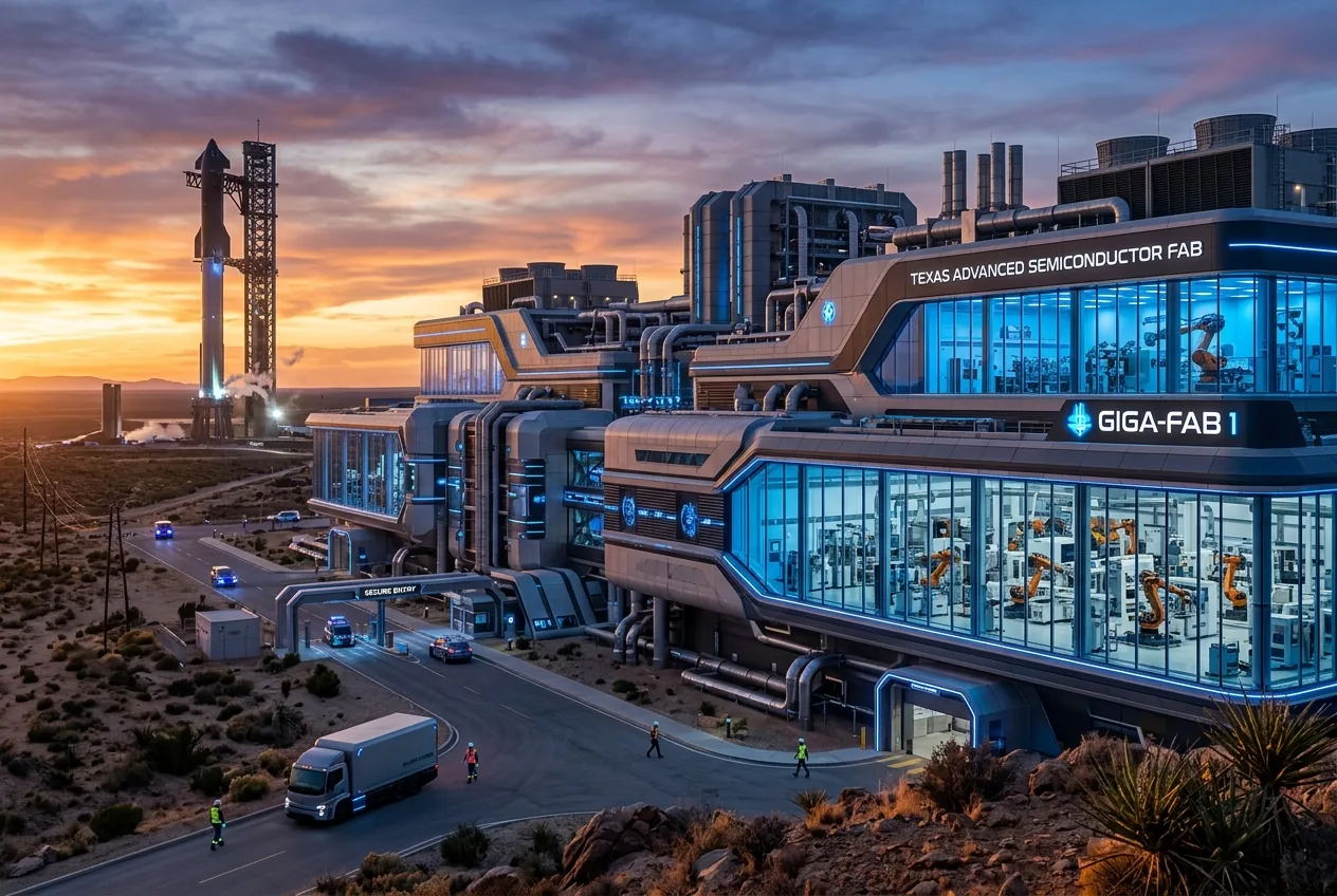
Intel CEO Lip-Bu Tan recently characterized the collaboration as a strategic alliance born of necessity. Musk’s vision across transportation and space travel requires an uninterrupted supply of silicon that can withstand harsh environments while performing trillions of operations per second. The Terafab project will reportedly consist of two primary fabrication plants in Austin. One facility is slated to focus on terrestrial applications—specifically the chips required for Tesla’s vehicle fleet and the evolving Optimus robot. The second facility is significantly more ambitious, targeting the production of chips for AI data centers located in space.
From a technical standpoint, the design requirements for these two categories of silicon are vastly different. Terrestrial robotics chips must prioritize low-latency inference and high energy efficiency to maximize the battery life of mobile units. Conversely, space-based chips must be radiation-hardened to survive the high-energy particles of the orbital environment while managing heat dissipation in a vacuum where convection is not an option. By co-locating the design and manufacturing capabilities for these disparate needs, the Terafab project aims to cross-pollinate the engineering breakthroughs required for both frontiers.
The One Terawatt Benchmark and Compute Density
The target of one terawatt of compute is a metric that shifts the conversation from transistor counts to total power throughput. In the context of xAI, Musk’s artificial intelligence venture, the need for massive compute clusters is immediate. Training large language models like Grok requires tens of thousands of GPUs working in parallel. However, as these models move toward “real-world AI”—processing live video feeds from millions of cameras or controlling complex robotic appendages—the hardware must shift from massive data centers to the edge.
Intel’s role in the Terafab project involves more than just etching silicon; it involves advanced packaging technologies like Foveros and EMIB (Embedded Multi-die Interconnect Bridge). These technologies allow for the stacking of chiplets, enabling higher compute density without a proportional increase in footprint. This is critical for the Optimus robot, where the “brain” must be compact enough to fit within a humanoid cranium while possessing the processing power to handle real-time balance, object recognition, and path planning. By leveraging Intel’s manufacturing prowess, the Terafab project can produce chips that are functionally customized for the mechanical constraints of the hardware they inhabit.
Why Texas Is the New Silicon Epicenter?
The $20 billion investment is expected to stimulate a massive secondary market for supply chain components, from specialized chemical suppliers to robotic assembly line manufacturers. For Intel, this project is a lifeline for its IDM 2.0 (Integrated Device Manufacturing) strategy, which seeks to open its factories to outside customers. Securing a client like Musk, who represents multiple high-growth sectors simultaneously, provides Intel with the consistent volume needed to refine its latest process nodes, such as the Intel 18A.
Solving the Robotics Latency Problem
One of the most significant challenges in modern robotics is the latency between sensor input and motor output. In a humanoid robot, even a few milliseconds of delay in the processing loop can result in a loss of equilibrium. Standard off-the-shelf processors often struggle with the specific mathematics required for inverse kinematics and spatial mapping. The Terafab initiative intends to “refactor silicon fab technology” to prioritize the specific data pathways used in neural network-based control systems.
Space-Hardened AI: The Orbiting Data Center
The second fab in the Austin complex focuses on a concept that sounds like science fiction but is a mechanical necessity for SpaceX’s future: orbital compute. As the Starlink constellation grows and SpaceX looks toward Mars, the need for high-level data processing in space becomes critical. Transmitting massive amounts of raw data back to Earth for processing creates a bandwidth bottleneck and introduces significant delay.
The solution is to put the AI in the satellite or the spacecraft itself. However, the vacuum of space is a brutal environment for electronics. The Terafab project aims to develop chips that use novel materials and architectures to mitigate the effects of cosmic radiation and thermal cycling. This requires a rethink of the physical packaging of the chip, potentially utilizing diamond substrates or specialized heat pipes integrated directly into the silicon carrier. Intel’s experience in high-reliability computing makes them an essential partner in this endeavor, providing the metallurgical and thermal engineering expertise that typical fabless chip designers lack.
The Economic Viability of the Terafab Gamble
Critics of the project point to the massive capital expenditure and the historical volatility of the semiconductor market. However, from an industrial perspective, the move is a defensive necessity. The global chip shortage of recent years proved that even the most advanced manufacturing lines can be brought to a halt by a lack of basic microcontrollers. By controlling the entire stack from the fab to the final robot or rocket, Musk is attempting to insulate his companies from future market shocks.
For Intel, the deal has already paid dividends in market confidence, with stock prices surging as investors recognize the potential of the Terafab as a cornerstone of the American silicon resurgence. The project is more than just a factory; it is a laboratory for the future of industrial automation. If successful, the Terafab will not only produce the chips that power the next generation of AI but will also establish a new blueprint for how technology companies and manufacturers can collaborate to solve the most difficult engineering problems of the 21st century.
As the first foundations are poured in Austin, the tech industry is watching closely. The Terafab project represents a convergence of interests between a legacy silicon giant and a disruptive industrialist. Whether it achieves the lofty goal of one terawatt of compute remains to be seen, but the technical and economic framework being laid today will undoubtedly influence the trajectory of robotics and aerospace for decades to come.

Comments
No comments yet. Be the first!